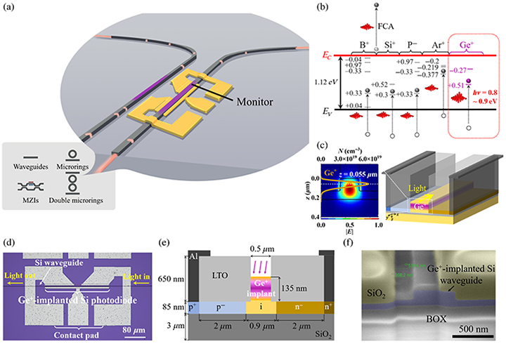
The NFF (CWB) user Yue NIU’s paper titled “Broadband sub-bandgap linear photodetection in Ge+-implanted silicon waveguide photodiode monitors” was published in the Advanced Photonics in September 2025. Yue NIU is supervised by Prof. Andrew W. POON.
This work presented a first Ge+-implanted silicon waveguide photodiode (PD) monitor operating in the dual-band spanning telecommunications O- and C-bands. Ge, a complementary metal-oxide-semiconductor-compatible group IV element, can substitute a silicon atom at a lattice site with minimal introduction of extra free carriers. They demonstrated responsivities of 124.8 mA ·W-1· mm-1 at 1310-nm wavelength (O-band) and of 31.2 mA · W-1 · mm-1 at 1550-nm wavelength (C-band), with a low dark current of 0.8 nA upon a small bias voltage of −3 V. The internal quantum efficiency exceeds that of B+-, P−-, and Ar+-implanted silicon PDs by factors of 4.9 to 16.8. The device exhibits optical absorption loss of < 0.012 dB · μm-1 and 98% linearity across < 1 mW on-chip power. Their Ge+-implanted silicon waveguide PDs hold significant promise in on-chip power monitors for programmable photonics. You can access the publication through this link.
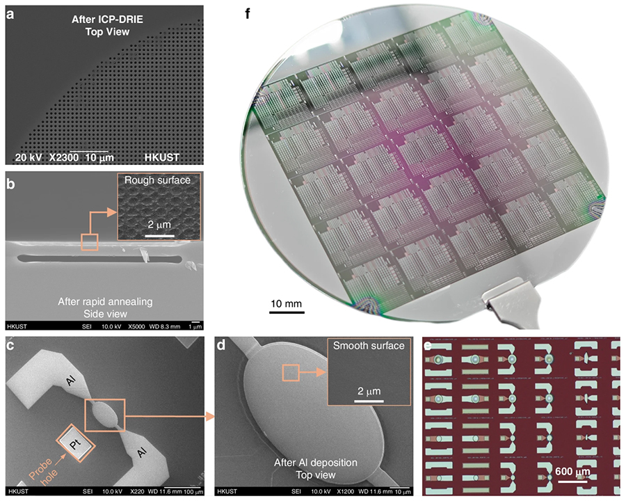
The NFF (CWB) user Jiashuai XU’s paper titled “A wafer-level sealed silicon cavity microacoustic platform for radio frequency integration” was published in the nature: microsystems & nanoengineering in May 2025. Jiashuai XU is supervised by Prof. Yansong YANG.
This study demonstrated a wafer-level sealed silicon cavity (SSC) microacoustic integration platform to address the limitations in the cavity Silicon-on-Insulator (C-SOI) wafers for the 5G/6G wireless communication system. The proposed SSC platform features an extremely smooth suspended membrane with adjustable thickness, flexible cavity shapes with high density, self-formed acoustic wave confinement steps, stable temperature coefficient of frequency (TCF), and highly integrated compatibility with complementary metal-oxide semiconductor (CMOS). A surface smoothing method based on wet oxidation for SSC wafers is presented, which achieves a root mean square (RMS) roughness on the cavity surface of 1.5 nm for the first time. Based on the presented SSC platform, an Al₀.₇₅Sc₀.₂₅N sealed cavity bulk acoustic wave resonator (S-BAR) is designed, fabricated, and characterized. The experimental results show that the asymmetric second-order (A2) Lamb mode of S-BAR is enhanced for higher frequency with a maximum piezoelectric coupling coefficient (kt²) of 9.53%, a maximum quality factor (Q) of 439, and a TCF of−11.44ppm/K. Different designs’ piezoelectric coupling coefficient distribution is consistent with the theoretical prediction. The proposed smoothing process increases the S-BARs’ quality factor by ~400%. The frequency shift caused by the temperature (absolute value of TCF) is reduced by 62% compared with the traditional Al₀.₇₅Sc₀.₂₅N thin film bulk acoustic wave resonator (without temperature compensation). The enhanced performances demonstrated the potential of SSC in the next-generation highly integrated RF communication systems. You can access the publication through this link.
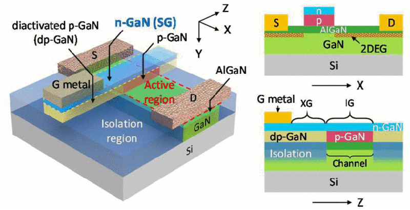
The paper by NFF (CWB) users Sirui FENG and Haochen ZHANG, titled “An All-GaN Semiconducting-Gate HEMT for Inherent Gate-Level High-Voltage Protection and Synchronous Switching with Photoelectrically Enhanced Conductivity” was published in the 2024 IEEE International Electron Devices Meeting (IEDM) in December 2024. Sirui FENG and Haochen ZHANG are supervised by Prof. Kevin J. CHEN.
They demonstrated a normally-off n-GaN/p-GaN/Al GaN/GaN HEMT featuring a semiconducting gate (SG), i.e., an n-GaN layer overlaying the 2DEG channel as an intrinsic gate and connected to an extrinsic electrode outside the active region. With an appropriate design, the n-GaN SG will be fully depleted when the 2DEG channel is sufficiently turned on, and thereby, decouples the vulnerable intrinsic gate stack from further increase in the extrinsic gate’s voltage. As a result, the SGHEMT can tolerate extremely high-voltage external gate transients (e.g., 500-μs pulses as high as 1.5 kV), enabling robust and reliable operations. Moreover, the SG structure allows using a peripheral 340-nm UV LED to create electron-hole pairs in the intrinsic gate stack. The resultant excessive holes could lead to higher 2DEG density in the channel, and thus, enhance the conductivity (reducing the on-resistance by 42.6%). With the LED driven synchronously with the gate-drive signal, the proposed SG-HEMT exhibits quick turn-off transients and immaterial changes to OFF-state characteristics. You can access the publication through this link.