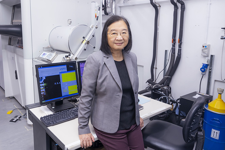
Twenty-six years ago, when I was planning the BIG move from the US to the city where I was born and grew up, Hong Kong, many friends from around the world were all curious about the reasons and asked if/when I would go back to the US. The answer is obvious for the second part – I am still happily enjoying my work and life in Hong Kong (UST) after 25 years.
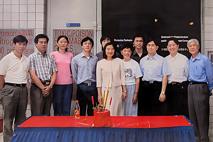
As for why moving to HKUST, one major reason is the well-facilitated Central Research Facilities on campus. I particularly appreciate the professionalism and experience of the NFF team. Before my move in the spring of 2000, the then NFF manager, Mr. Gen CHIN paid me a visit at my former institution and lab, to get an understanding of the nature of my research and needs. After I arrived in the summer of 2000, Mr. CHIN showed me the ropes how to work with various departments of the University and the HK government, to secure our approval (license) of using electronic specialty gases and chemicals for epitaxial growth. We successfully established the MOCVD lab in NFF Phase I (now named PTC) in a timely and smooth manner. This photo was taken during the opening ceremony of my MOCVD lab in 2002.
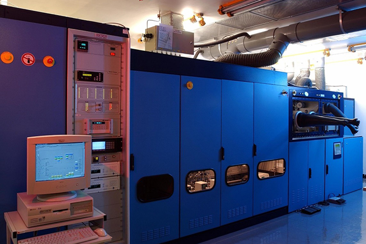
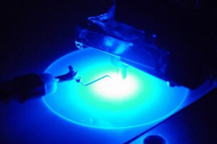
As my research program focuses on III-V materials and devices, fabrication of devices with our designs and epi-layers is of critical importance. The device fabrication facilities in NFF Phase II and III (also named NFF Enterprise Center) allow us to realize our research over the past 25 years. I was an early explorer of the development of monolithic integration of semiconductor devices and systems on industry-standard silicon substrates by MOCVD. MY group was the first to demonstrate the highest mobility and millimeter-wave III-V transistors that are lattice-matched to InP grown directly on Si. Additionally, we led the development of the first 1.5 µm room-temperature electrically pumped III-V quantum dot lasers epitaxially grown on CMOS-standard (001) Si substrate by MOCVD. Recently, my group developed the lateral aspect ratio trapping (LART) technique to grow III-V active devices in the same plane as the Si layer, enabling efficient coupling with Si waveguides on silicon-on-insulator (SOI). I also invented the LED-on-Silicon (LEDoS) - an groundbreaking array of LEDs addressable with a silicon active matrix, enabling high-resolution micro-displays visible under bright daylight. Our patented LEDoS monolithic micro-LED arrays driven by a CMOS backplane have been commercialized for smart glass applications with full-color micro-displays. Furthermore, our group has also been investigating the growth of GaN vertical trench MOSs on foreign and native substrates for high-performance power devices. Without the equipment and the professional technical support provided by NFF, none of these achievements would have been possible. NFF has also played a crucial role in the hands-on training of all my group members.

Postgraduates from our group, Photonics Technology Center (PTC) are all well trained to carry out experimental work. These researchers are now carrying on the torch in various universities, labs, and industries around the world, thanks to their particularly hands-on experience in NFF.
NFF not only strengthened my academic career in the past two decades but also nurtured many PTCers and put HKUST on the world map of compound semiconductor materials and devices.