Research on Flexible Electronics
Prof. Hongyu YU of the Department of Mechanical and Aerospace Engineering (MAE) of the HKUST focuses on designing and fabricating origami or metastructure-enabled flexible devices and electronics in all macro-scale, micro-scale, and nano-scale levels. Origami structures, typically wavy structures and Miura-ori structures are natural stretchable structures that can help endow otherwise rigid or non-stretchable material with good stretchability. Origami designs are also used for exotic material properties, such as increasing mechanical strength or for sound absorption.
At present, most of Prof. Hongyu YU's group members are NFF(CWB) users, and fabrication processes - including all silicon wafer machining processes in MEMs and silicone rubber (PDMS or Ecoflex) preparation - are finished in NFF(CWB). Some highlighted research works, including stretchable origami-shaped wires and conductors, programmable designed shape conformable LED displays, and stretchable transparent strain sensors fabricated in NFF(CWB), are summarized below.

A biaxially stretchable LED display based on wavy structured metal electrode grid packaged together with LED chips is demonstrated. The MEMS fabrication process was utilized to fabricate the wavy-structured metal connections and rigid islands. The resulting LED display can be readily bent, rolled, stretched and even washed with no degradation of its image quality. Furthermore, at least 1000 stretching cycles at 10% strain can be tolerated. This work demonstrates the potential of inorganic materials as stretchable displays and MEMS-compatible processes as stretchable electronics fabrication processes.

Wavy-structured metal grid enabled flexible electronics. (a) Photograph of the assembled display with all LED chips lit up; (b) Scanning electronic microscope (SEM) photograph of the wavy model’s top view; (c) SEM photograph of the wavy model’s side view.
A biaxially stretchable LED display based on wavy structured metal electrode grid packaged together with LED chips is demonstrated. The MEMS fabrication process was utilized to fabricate the wavy-structured metal connections and rigid islands. The resulting LED display can be readily bent, rolled, stretched and even washed with no degradation of its image quality. Furthermore, at least 1000 stretching cycles at 10% strain can be tolerated. This work demonstrates the potential of inorganic materials as stretchable displays and MEMS-compatible processes as stretchable electronics fabrication processes.
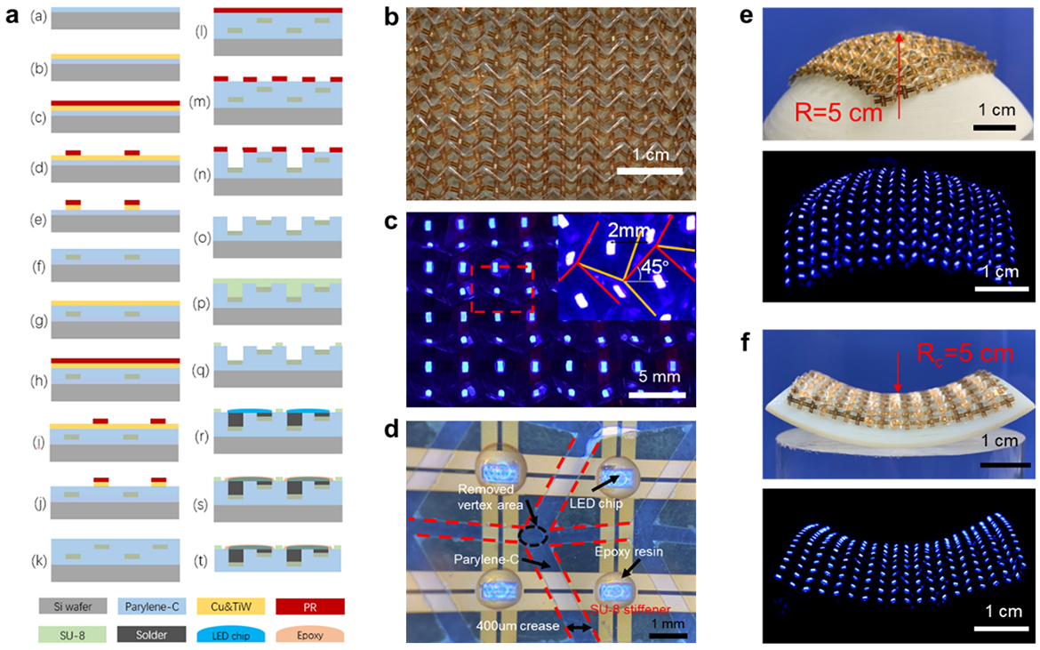
By taking the bending stiffness of facets into consideration, a different approach through the design of Miura-like origami tessellations that can be folded into nondevelopable surfaces with minimal in-facet bending and that remain compatible with existing high-throughput manufacturing processes has been developed. The optimization the algorithm minimizes the pseudo strain energy of all facets, thus minimizing the deformation on the facets of origami during folding. A special finite element scheme is used to calculate the weak-form functional extremum in classical differential geometry and helps programmatically design the specific 2D origami pattern. The silicon-based microfabrication process, pick-and-place packaging process, and mold-based origami folding process are integrated for manufacturing curved LED displays of nondevelopable surfaces, such as spherical and saddle surfaces.

By taking the bending stiffness of facets into consideration in this study, a different approach has been developed through the design of Miura-like origami tessellations that can be folded into nondevelopable surfaces with minimal in-facet bending and remain compatible with existing high-throughput manufacturing processes. The optimized algorithm minimizes the pseudo strain energy of all facets, thus minimizing the deformation on the facets of origami during folding. A special finite element scheme is used to calculate the weak-form functional extremum in classical differential geometry and helps programmatically design the specific 2D origami pattern. The silicon-based microfabrication process, pick-and-place packaging process, and mold-based origami folding process are integrated for manufacturing curved LED displays of nondevelopable surfaces, such as spherical and saddle surfaces.