Publication Highlights
NFF (CWB) user Dr. Hanke FENG’s paper tilted “Integrated lithium niobate microwave photonic processing engine” was published in the Nature in February 2024. Dr. Hanke FENG is supervised by Prof. Cheng WANG from the Department of Electrical Engineering at the City University of Hong Kong.
This work demonstrates such an integrated MWP processing engine based on a 4-inch wafer-scale thin-film lithium niobate platform. It can perform multipurpose tasks with processing bandwidths of up to 67 GHz at complementary metal–oxide–semiconductor (CMOS)-compatible voltages. They achieve ultrafast analogue computation, namely temporal integration and differentiation, at sampling rates of up to 256 giga samples per second, and deploy these functions to showcase three proof-of-concept applications: solving ordinary differential equations, generating ultra-wideband signals and detecting edges in images. They further leverage the image edge detector to realize a photonic-assisted image segmentation model that can effectively outline the boundaries of melanoma lesion in medical diagnostic images. Our ultrafast lithium niobate MWP engine could provide compact, low-latency and cost-effective solutions for future wireless communications, high-resolution radar and photonic artificial intelligence. You can access the publication through this link.

NFF (CWB) user Dr. Hanke FENG’s paper tilted “Integrated lithium niobate microwave photonic processing engine” was published in the Nature in February 2024. Dr. Hanke FENG is supervised by Prof. Cheng WANG from the Department of Electrical Engineering at the City University of Hong Kong.
This work demonstrates such an integrated MWP processing engine based on a 4 inch wafer-scale thin-film lithium niobate platform. It can perform multipurpose tasks with processing bandwidths of up to 67 GHz at complementary metal–oxide–semiconductor (CMOS)-compatible voltages. They achieve ultrafast analogue computation, namely temporal integration and differentiation, at sampling rates of up to 256 giga samples per second, and deploy these functions to showcase three proof-of-concept applications: solving ordinary differential equations, generating ultra-wideband signals and detecting edges in images. They further leverage the image edge detector to realize a photonic-assisted image segmentation model that can effectively outline the boundaries of melanoma lesion in medical diagnostic images. Our ultrafast lithium niobate MWP engine could provide compact, low-latency and cost-effective solutions for future wireless communications, high-resolution radar and photonic artificial intelligence. You can access the publication through this link.

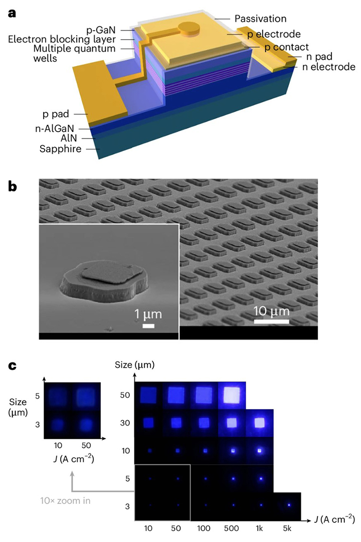
NFF (CWB) user Dr. Feng FENG’s paper titled “High-power AlGaN deep-ultraviolet micro-light-emitting diode displays for maskless photolithography” was published in the nature photonics in September 2024. Dr. Feng FENG is supervised by Prof. Hoi-Sing KWOK and Prof. Zhaojun LIU.
In this study, advanced fabrication processes have been developed to enable the demonstration of highly efficient 270 nm UVC micro-LEDs and large-format UVC micro-LED displays with high resolution for maskless photolithography. Optical and electrical characterizations were performed on UVC micro-LEDs with sizes ranging from 3 µm to 100 μm to evaluate these emerging devices. The 3 μm device achieved a record-high peak external quantum efficiency of 5.7% and a maximum brightness of 396 W cm–2. Moreover, 2,540 pixels per inch parallel-connected UVC micro-LED arrays featuring rear-side reflection layers exhibited emission uniformity and collimation. UVC micro-LED displays, with a resolution of 320 × 140, were explicitly designed for maskless photolithography applications utilizing a customized integrated circuit driver for optimal performance. The UVC micro-LEDs and UVC micro-displays provide sufficient doses to fully expose the photoresist film within seconds, owing to their enhanced current spreading uniformity, improved heat dispersion and superior light extraction efficiency. This work may open a path to maskless photolithography, potentially leading to revolutionary developments in the semiconductor industry. You can access the publication through this link.

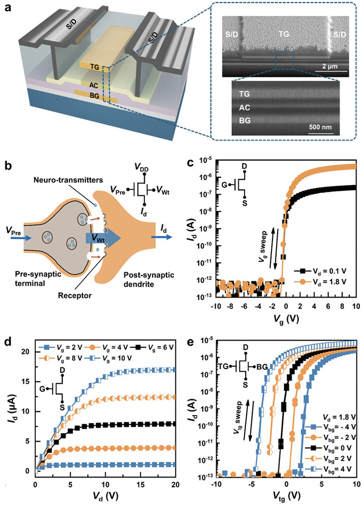
NFF (CWB) user Prof. Yushen HU’s paper titled “A Sliding-Kernel Computation-In-Memory Architecture for Convolutional Neural Network” was published in the Advanced Science in October 2024. Prof. Yushen HU is co-worked with Prof. Man WONG.
This work reported a sliding-kernel computation-in-memory (SKCIM) architecture conceptually involving two overlapping layers of functional arrays, one containing memory elements and artificial synapses for neuromorphic computation, the other is used for storing and sliding convolutional kernel matrices. A low-temperature metal-oxide thin-film transistor (TFT) technology capable of monolithically integrating single-gate TFTs, dual-gate TFTs, and memory capacitors is deployed for the construction of a physical SKCIM system. Exhibiting an 88% reduction in memory access operations compared to state-of-the-art systems, a 32 × 32 SKCIM system is applied to execute common convolution tasks. A more involved demonstration is the application of a 5-layer, SKCIM-based convolutional neural network to the classification of the modified national institute of standards and technology (MNIST) dataset of handwritten numerals, achieving an accuracy rate of over 95%. You can access the publication through this link.
