Publication Highlights
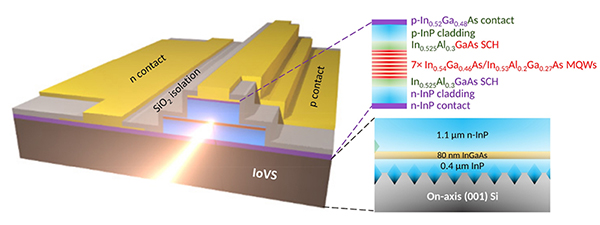
NFF user, Si ZHU’s paper titled “Room-temperature electrically-pumped 1.5 μm InGaAs/InAlGaAs laser monolithically grown on on-axis (001) Si” was featured in Semiconductor TODAY: Monolithic indium phosphide on silicon growth for optoelectronics, in June 2018. Si ZHU is supervised by Prof. Kei May LAU.
It is the first indium gallium arsenide/indium aluminum gallium arsenide (InGaAs/InAlGaAs) multi-quantum-well (MQW) lasers directly grown on an on-axis V-grooved (001) Si substrate by metal-organic chemical vapor deposition (MOCVD). Monolithic integration, it is hoped, will reduce the costs arising from additional processing needed for wafer bonding, and also allow the use of larger-diameter substrates for economies of scale.
Lasing near 1.5 μm from lasers that were monolithically grown on silicon was achieved for the first time, with a threshold current density Jth = 3.3 kA/cm2 under a pulsed current injection at room temperature. The results demonstrate the potential of adopting such a large-area InP-on-Si substrate for integrating diverse III-V laser diodes, photodetectors, high-frequency and high-speed transistors.

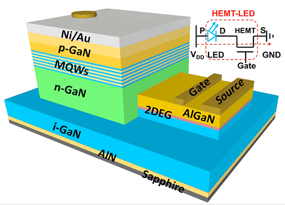
NFF user, Yuefei CAI’s paper titled “Voltage-Controlled GaN HEMT-LED Devices as Fast-Switching and Dimmable Light Emitters” was featured in IEEE Spectrum: New Device Could Drive MicroLED Displays, Li-Fi in Feb. 2018. Yuefei CAI is supervised by Prof. Kei May LAU.
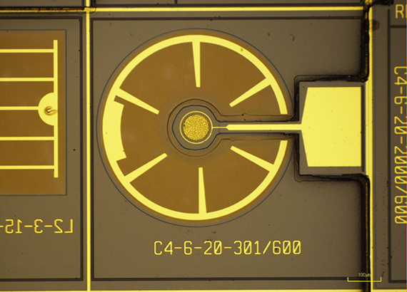
HEMT-LED devices could make upcoming microLED displays easier to engineer and visible-light communications systems, like LiFi, faster. The HEMT-LED, which is a bit like a light-emitting transistor, let you switch light emission on and off and control the brightness with voltage signals. Prof. Lau’s lab has been focusing on making arrays of small HEMT-LEDs, with the goal to incorporating them in microLED displays. The device shows an enormous potential for visible-light communications. It might be used for Li-Fi, vehicle-to-vehicle communications via headlights, and other schemes in the future.

