Events and Activities
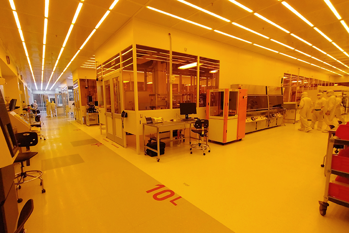
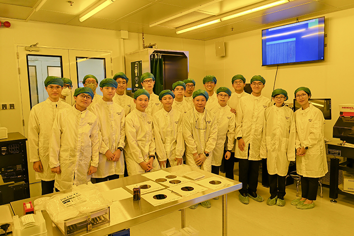
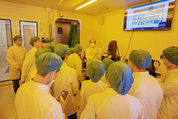
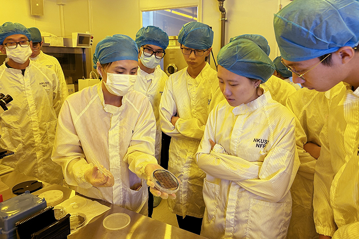
Since January of this year, we have organized more than 50 engaging lab visits and sessions, providing an opportunity for participants to explore our facilities and learn about our research initiatives. These visits have served hundreds of visitors from various parties, such as secondary schools, private companies, and the government sector.
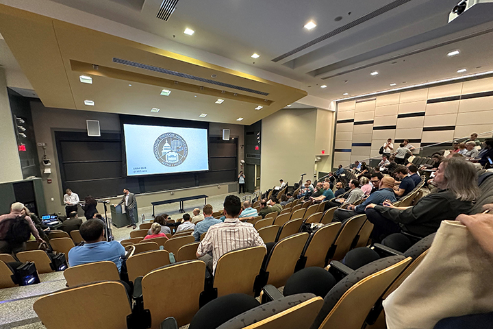
This year, UGIM 2024 was held at MIT (The Massachusetts Institute of Technology) from June 23rd to June 26th, 2024. NFF (CWB) participated in the symposium, which brings together operators, managers, and administrators of university facilities involved in micro/nanotechnology fabrication and characterization from around the world. The event provides a valuable forum for exchanging information on a wide range of topics. A key highlight of the symposium was a visit to MIT.nano cleanroom, a newly constructed 200,000-square-foot research facility dedicated to nanoscience and nanotechnology.
